


 Support Center
Understanding The Digital Image Sensor
While a sensor's function is to convert light into an electrical signal, not all sensors are
built the same. Learning more about how image sensors work and how they are categorized
will help you better choose the right one.
Understanding The Digital Image Sensor
However they are classified, the purpose of image sensors are the same; to convert incoming light (photons) into an electrical signal that can be viewed, analyzed, or stored. Image sensors are a solid-state device and serve as one of the most important components inside a machine vision camera. Every year new varieties of sensors are manufactured with improvements to sensor size, resolution, speed, and light sensitivity. In this article we discuss some of the basics of image sensor technology found inside machine vision cameras and how those relate to their classifications.
Table of Contents
Image Sensor Components
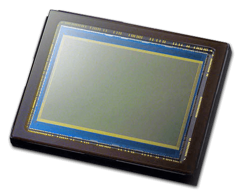
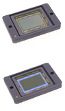
Below is a typical CMOS image sensor. The sensor chip is held in a package with protective glass. The package has contact pads which connect the sensor to the PCB.
Side Note
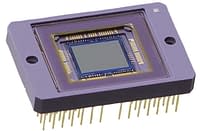
Different sensors come in different packages. For example, the above photo is a sensor with a ceramic PGA package.
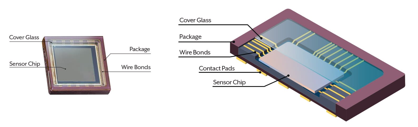
Above: Diagram of a CMOS Image Sensor
The solid-state image sensor chip contains pixels which are made up of light sensitive elements, micro lenses, and micro electrical components. The chips are manufactured by semiconductor companies and cut from wafers. The wire bonds transfer the signal from the die to the contact pads at the back of the sensor. The packaging protects the sensor chip and wire bonds from physical and environmental harm, provides thermal dissipation, and includes interconnecting electronics for signal transfer. A transparent window in the front of the packaging called a cover glass protects the sensor chip and wires while allowing light to reach the light sensitive area.
Image Sensors from Silicon Wafers
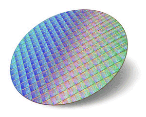
Sensor dies are produced in large batches on silicon wafers. The wafers are cut into many pieces with each piece housing a single sensor die. The larger the sensor die size, the lower number of sensors per wafer. This typically leads to higher costs. A single defect on a wafer will have a higher probability of impacting a larger image sensor.

Above: Sensor Dies Are Removed From The Wafer With Precision Cutting
Side Note
 The manufacturing process from bare silicon wafer to individual image sensor pieces may take up to several months.
Sensor Functions Inside a Camera
In a camera system, the image sensor receives incident light (photons) that is focused through a lens or other optics. Depending on whether the sensor is CCD or CMOS, it will transfer information to the next stage as either a voltage or a digital signal. CMOS sensors convert photons into electrons, then to a voltage, and then into a digital value using an on-chip Analog to Digital Converter (ADC).
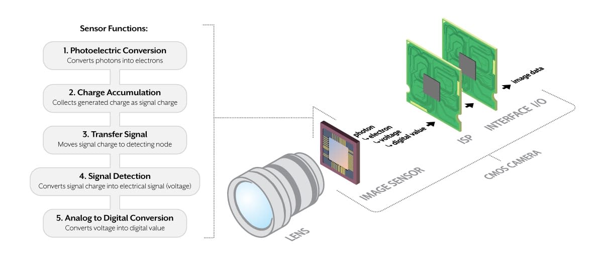
Above: Typical CMOS Camera Layout.
Depending on the camera manufacturer the general layout and components used will differ. The main purpose of this layout is to convert light into a digital signal which can then be analyzed to trigger some future action. Consumer level cameras would have additional components for image storage (memory card), viewing (embedded LCD) and control knobs and switches that machine vision cameras do not.
Differences Between CCD and CMOS
CCD sensors (Charged Couple Device) start and stop exposure for all pixels at the same time. This is known as global shutter. The CCD then tranfers this exposure charge to the horizontal shift register where it is then sent to the floating diffusion amplifier. Note: In 2015, Sony announced plans to discontinuing their CCD production and end support for CCDs by 2026.

CCD characteristics:
• Global shutter
• Low noise
• High dynamic range
• Medium range frame rates
• Subject to smearing
In the past, CMOS sensors (Complementary Metal-Oxide Semiconductor) were only able to start and stop exposure one pixel row at a time, which is known as rolling shutter. This has changed over time, with many global shutter CMOS sensors now available in the market. CMOS sensors use smaller ADCs for each pixel column allowing for higher frame rates than CCDs. CMOS sensors have undergone major improvements over the years making most modern CMOS sensors equal or superior to CCDs for image quality, image speed, and overall value.

 Modern CMOS characteristics:
• Global shutter and rolling shutter models
• Low to very low noise
• High to very high dynamic range
• Very high frame rates
• No smearing
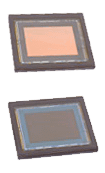
Mono and Color Sensors
For visible light sensors (not infrared, UV, or X-Ray) there are two main types; color and mono. Color sensors have an extra layer that sits below the micro lens, called a color filter, which absorbs undesired color wavelengths so that each pixel is sensitive to a specific color wavelength. For mono sensors, there is no color filter so each pixel is sensitive to all visible light wavelengths.

Above Left: Mono Sensor Plane. Above Right: Color Sensor Plane with Bayer Pattern.
For the color sensor example shown above right, the color filter array employed is a Bayer filter pattern. This filter pattern uses a 50% green, 25% red and 25% blue array. While most color cameras use the Bayer filter pattern, there are other filter patterns available that have different pattern arrangements and RGB breakdowns.
Side Note
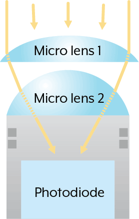
For some sensors, especially sensors with smaller pixel sizes, additional micro lenses are used to help guide photons into the photodiode.
Image Sensor Format (Size)
Image sensors come in different format types (also known as optical class, sensor size or type) and packages. Resolution and pixel size will dictate the overall size of a sensor with larger sensors having either higher resolutions or larger pixel sizes than smaller sensors. Knowing the sensor format is important for choosing a lens and optics for a camera. All lenses are designed for specific sensor formats and resolutions. Note that sensor formats only describe the area of the sensor chip and not the entire sensor package.
Above, Sensor Format Sizes (Left to Right): 1/6″, 1/3″, 2/3″, 1″
Below is an example of a CMOS sensor that is categorized with a format type of 2/3″. However, the actual diagonal size of the die is only 0.43″ (11mm). Current sensor “inch” types are NOT the actual diagonal size of the sensor. While it may seem that sensor format types are somewhat ambiguously defined, it is actually based on old video camera tubes where the inch measurement referred to the outer diameter of the video tube. Below shows a chart with the most common sensor format types and their real sensor diagonal sizes in mm.
Side Note
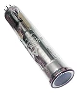
Here is an example of an old video camera tube. The diameter of these old tubes serve as the sensor format classification for today’s modern sensors.

Sensor Format vs. Actual Size
| Image Sensor Format (Type) | 1" | 2/3" | 1/1.8" | 1/3" |
| Image Sensor Diagonal (mm) | 16 mm | 11 mm | 8.9 mm | ~6 mm |
Sensor Pixel Size
Pixel size is measured in micrometers (µm) and includes the entire area of both the photodiode and surrounding electronics. A CMOS pixel consists of a photodiode, an amplifier, reset gate, transfer gate and floating diffusion. These elements however may not always be within each pixel as they can also be shared between pixels. The diagram below shows a simplified layout of a CMOS mono and color pixel.
Above, Simplified CMOS Mono & Color Pixel Layout
Typically a larger pixel size is better for increased light sensitivity because there is more area of the photodiode to receive light. If the sensor format stays the same but the resolution increases the pixel size must decrease. While this might decrease sensor sensitivity, improvements in pixel structure, noise reduction technology, and image processing have helped mitigate this. To get a more accurate understanding of sensor sensitivity it is best to refer to the sensor’s spectral response (quantum efficiency) as well as other sensor performance results.
Mono & Color Spectral Response
Because of the physical differences between a mono and color sensors, as well as the differences between a sensor manufacturer’s technologies and pixel structure, different sensors will sense light to varying degrees. One way to get a more accurate understanding of a sensor’s sensitivity to light is by reading its spectral response chart (also known as a Quantum Efficiency Chart).
The 2 charts below are the mono and color versions of the same sensor model. The left shows the spectral response of a mono sensor and the right of a color sensor. The X axis is the wavelength (nm) and the Y axis is quantum efficiency (%). The majority of machine vision color cameras have IR cut filters installed to block near-IR wavelengths. This removes IR noise and color cross-over from the image, best matching how the human eye interprets color. However, in a number of applications it can be beneficial to image without the IR cut filter. Whether or not an IR cut filter is installed a color sensor will never be as sensitive as the mono sensor.

Above: 2 Spectral Response Curves Examples Using Same Sensor Family.
Mono Sensor (Left) and Color Sensor With No IR Cut Filter (Right)
The higher the quantum efficiency the better the sensor is at sensing light. The above charts are one of many performance results based on the measurement standards of EMVA 1288. The EMVA 1288 standard dictates how to test and display performance results so that users can better compare and contrast models across vendors. Visit the EMVA 1288 site for more information.
Global versus Rolling Shutter
An important function of the sensor is its shutter type. The two main electronic shutter types are global shutter and rolling shutter. These shutter types are different in their operation and final imaging results, especially when the camera or target is in motion. Let’s look in detail at how they work and how this affects imaging.
Global Shutter Timing
The diagram to the left shows the exposure timing of a global shutter sensor. All pixels begin and end exposure at the same time but readout still happens line by line. This timing produces non-distorted images without wobble or skewing. Global shutter sensors are essential for imaging high speed moving objects.

Rolling Shutter Timing

The diagram to the left shows the exposure timing of a rolling shutter sensor. Exposure timing is different line by line with reset and readout happening at shifted times. This row by row exposure produces image distortion if either the target or camera are in motion. Rolling shutter sensors offer excellent sensitivity for imaging static or slow moving objects.

Conclusion
If you’re just beginning to explore the world of machine vision cameras the above information is an excellent start in understanding how the machine vision industry categorizes sensors. Understanding the terms and technology in digital sensors will allow you to better pinpoint the appropriate camera for your application. For example, certain sensor specifications, such as pixel size and sensor format, will play an important role in choosing the correct lens. In addition, as new sensor technologies emerge you’ll be better equipped in understanding if it is beneficial to your application. If you are ready to discuss your camera requirements, please contact our knowledgeable Lucid sales staff.